← SG3525 Inverter Circuit Diagram PDF: Desain Inverter Sine Wave yang Andal! sg3525 pwm ic pinout, examples, applications, features,, 55% off Wiring Diagram for a Kenwood: Upgrade Your Car Stereo System! Three phase electrical wiring installation in home →
If you are looking for PCB Design Layout | ROJ you've came to the right web. We have 25 Pics about PCB Design Layout | ROJ like PCB Layout Design | PDF, PCB Layout Design Tips - Grounding Considerations - OnElectronTech and also PCB Layout Design | PDF. Here it is:
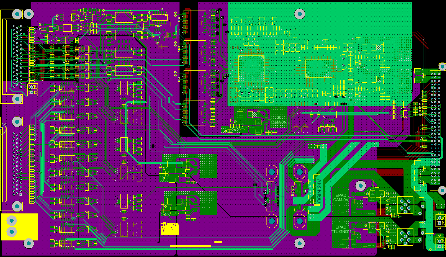
PCB Design Layout | ROJ
 roj.com
PCB Design Layout | ROJ
PCB Design Best Practices And Layout Guidelines | Cadence
 resources.pcb.cadence.com
PCB Design Best Practices and Layout Guidelines | Cadence
Basic Steps To Design A PCB Layout – PCB HERO
 www.pcb-hero.com
Basic Steps to Design a PCB Layout – PCB HERO
Best Practices In PCB Design | PDF | Printed Circuit Board | Computer
 www.scribd.com
Best Practices in PCB Design | PDF | Printed Circuit Board | Computer ...
PCB Layout Design Tips - Grounding Considerations - OnElectronTech
 www.scribd.com
PCB Layout Design Tips - Grounding Considerations - OnElectronTech ...
A Detailed Guide To PCB Layout Design - IBE Electronics
 www.pcbaaa.com
A detailed guide to PCB layout design - IBE Electronics
Practical PCB Layout Tips Every Designer Needs To Know
 www.scribd.com
Practical PCB Layout Tips Every Designer Needs to Know
PCB Design & Layout Skills – PCB Manufacturing And PCBA Assembly
 www.grande-pcba.com
PCB Design & Layout Skills – PCB Manufacturing and PCBA Assembly ...
PCB Design Best Practices And Layout Guidelines | Cadence
 resources.pcb.cadence.com
PCB Design Best Practices and Layout Guidelines | Cadence
PCB Layout Services – Electronics Engineering Design Services
 www.microelectronicos.net
PCB Layout Services – Electronics Engineering Design Services
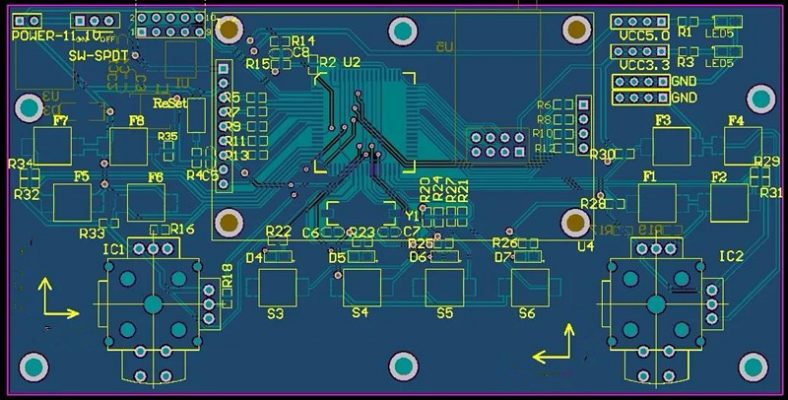
PCB Layout Design | PDF
 www.scribd.com
PCB Layout Design | PDF
PCB Layout Services – Electronics Engineering Design Services
 www.microelectronicos.net
PCB Layout Services – Electronics Engineering Design Services
PCB Design Best Practices And Layout Guidelines | Cadence
 resources.pcb.cadence.com
PCB Design Best Practices and Layout Guidelines | Cadence
PCB Layout Services| PCB Prototype | Reverse Engineering
 gespcb.com
PCB Layout Services| PCB Prototype | Reverse Engineering
Guide To PCB Design | PDF | Computer Engineering | Electrical Engineering
 www.scribd.com
Guide to PCB Design | PDF | Computer Engineering | Electrical Engineering
PCB Layout Design - Proescircuits
 proescircuits.com
PCB Layout Design - proescircuits
Practical PCB Layout Tips Every Designer Needs To Know - Technical Articles
.jpg) www.allaboutcircuits.com
www.allaboutcircuits.com
Practical PCB Layout Tips Every Designer Needs to Know - Technical Articles
PCB Layout Design: Techniques For Grid Settings - Andwin
 www.andwinpcba.com
PCB Layout Design: Techniques for Grid Settings - Andwin
A Detailed Guide To PCB Layout Design - IBE Electronics
 www.pcbaaa.com
A detailed guide to PCB layout design - IBE Electronics
PCB Design & Layout Skills – PCB Manufacturing And PCBA Assembly
 www.grande-pcba.com
PCB Design & Layout Skills – PCB Manufacturing and PCBA Assembly ...
PCB Layout Design – Twinkle Technology
 twinkle.com.my
PCB Layout Design – Twinkle Technology
Essential PCB Design/Layout Techniques: Final Part Now Available - EMC
 www.emcstandards.co.uk
Essential PCB Design/Layout Techniques: Final Part Now Available - EMC ...
PCB Design & Layout
 www.truelancer.com
PCB Design & Layout
PCB Layout Services| PCB Prototype | Reverse Engineering
 gespcb.com
PCB Layout Services| PCB Prototype | Reverse Engineering
Maximizing High-Speed Signal Integrity: Advanced PCB Layout Techniques
 86pcb.com
Maximizing High-Speed Signal Integrity: Advanced PCB Layout Techniques ...
Guide to pcb design. A detailed guide to pcb layout design. pcb design & layout skills – pcb manufacturing and pcba assembly ...